TL;DR
Intel has commenced shipping silicon wafers produced using high-NA EUV lithography. This development could enhance chip performance and manufacturing efficiency. The move signifies progress in advanced semiconductor fabrication but details on volume and customer deployment remain limited.
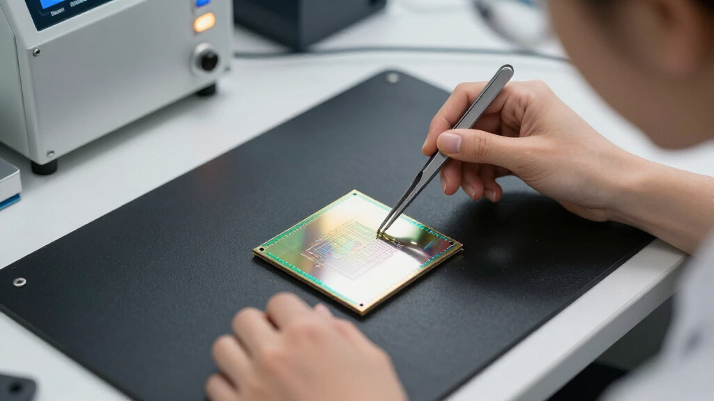
Intel has started shipping silicon wafers manufactured using high-NA EUV lithography technology, marking a major milestone in the company’s advanced chip production capabilities. This development is significant because high-NA EUV allows for smaller feature sizes and improved transistor performance, which are critical for next-generation processors. The move underscores Intel’s progress in semiconductor manufacturing and its efforts to stay competitive in the industry.
Intel announced that it has begun shipping silicon wafers produced with high-NA EUV (extreme ultraviolet) lithography technology. This process involves using a higher numerical aperture (NA) in EUV tools, which enables finer patterning at smaller nodes, potentially below 2 nanometers. The shipments include wafers intended for both internal testing and select customer evaluation, according to Intel officials.
High-NA EUV technology represents a significant leap over previous EUV systems, offering greater resolution and patterning precision. Intel has been investing heavily in this technology over the past several years, aiming to overcome limitations faced by traditional EUV tools at advanced nodes. The company claims that this move will enhance transistor density, improve power efficiency, and support future chip architectures.
While Intel has confirmed the start of shipments, it has not disclosed specific quantities, customer details, or production volumes. Industry analysts suggest that this step indicates Intel’s readiness to incorporate high-NA EUV into its mainstream manufacturing process, possibly starting with its upcoming process node, Intel 20A, expected to debut in 2024 or 2025.
Potential Impact of High-NA EUV on Chip Manufacturing
The shipping of high-NA EUV wafers by Intel marks a critical advancement in semiconductor manufacturing technology. This process enables the production of smaller, more powerful, and energy-efficient chips, which are essential for high-performance computing, AI, and mobile devices. For Intel, this move could help close the gap with competitors like TSMC and Samsung, who are also investing in advanced EUV techniques. For the broader industry, it signals a shift toward more widespread adoption of high-NA EUV, potentially accelerating Moore’s Law at the manufacturing level.
high-NA EUV lithography semiconductor equipment
As an affiliate, we earn on qualifying purchases.
As an affiliate, we earn on qualifying purchases.
Background on EUV and Semiconductor Fabrication Progress
Extreme ultraviolet lithography has been a key focus in semiconductor manufacturing for over a decade, aiming to enable smaller feature sizes than traditional optical lithography allows. Intel has been developing EUV technology for several years, with initial deployments at the 7nm and 5nm nodes. High-NA EUV, characterized by a higher numerical aperture, has been considered the next step to push beyond current limits.
Previous EUV tools, with NA around 0.33, faced challenges in patterning at the most advanced nodes, leading manufacturers to seek higher-NA systems. Major equipment vendors like ASML have been developing high-NA EUV tools, with commercial availability expected in the next few years. Intel’s move to ship wafers with high-NA EUV marks a significant milestone in this ongoing industry transition.
Intel’s investment in this technology aligns with its roadmap to produce chips at sub-2nm nodes, aiming for performance gains and power efficiency improvements vital for future computing demands.
“We are pleased to announce that we have begun shipping wafers produced with high-NA EUV technology, a key step toward next-generation manufacturing processes.”
— Intel spokesperson
Intel silicon wafer shipping
As an affiliate, we earn on qualifying purchases.
As an affiliate, we earn on qualifying purchases.
Uncertainties About Production Scale and Deployment
It is not yet clear how many wafers Intel plans to produce with high-NA EUV or when this technology will be incorporated into mass production for commercial chips. Details on customer adoption, specific process nodes, and potential cost implications remain undisclosed. Industry sources suggest that widespread deployment might still be several quarters away, pending further process refinement and equipment availability.
advanced EUV lithography tools
As an affiliate, we earn on qualifying purchases.
As an affiliate, we earn on qualifying purchases.
Upcoming Steps Toward Commercial Adoption
Intel is expected to continue testing and qualifying high-NA EUV wafers, with plans to integrate this technology into its next-generation process nodes, potentially starting with Intel 20A. The company may also begin shipping high-NA EUV wafers to select customers for evaluation. Industry observers will watch for official statements on production volumes and timelines for full commercial rollout.

INSILICON'S JPEG2000 ENCODER ACCELERATES AND OPTIMIZES NEXT GENERATION IMAGE COMPRESSION.(Product Announcement): An article from: EDP Weekly's IT Monitor
As an affiliate, we earn on qualifying purchases.
As an affiliate, we earn on qualifying purchases.
Key Questions
What is high-NA EUV lithography?
High-NA EUV lithography uses a higher numerical aperture in EUV tools, allowing for finer patterning at smaller feature sizes, essential for advanced semiconductor nodes.
Why is this development important for Intel?
It demonstrates Intel’s progress in adopting cutting-edge manufacturing technology, which can lead to more powerful, efficient chips and help it compete with other industry leaders.
When might high-NA EUV be used in mass production?
Industry estimates suggest full integration into mass manufacturing could occur within the next 1-2 years, starting with flagship process nodes.
What companies are involved in developing high-NA EUV technology?
Intel is developing and shipping wafers with high-NA EUV; equipment vendor ASML is manufacturing the high-NA EUV tools expected to be used in this process.
Will this impact chip prices or availability?
Potentially, as advanced manufacturing can increase costs initially, but improved efficiency and performance could benefit consumers in the long run. The exact impact remains uncertain at this stage.
Source: hn